Electric Circuits
To learn about the concept of capacitance, resistance and inductance; and about the phenomenon of (electrical) resonance.
This prelab homework must be done at home and handed to the lab TA before you start the lab. Read the instructions for this lab and consult the course textbook for relevant sections.
This will be accomplished by first studying RC circuits and then resonant RLC circuits. To do this, you will first quickly review the use of an oscilloscope, the most versatile electronic measuring instrument. Then you will use this tool to investigate the characteristics of capacitors and resonant circuits.
An oscilloscope is an instrument principally used to display signals as a function of time. With an oscilloscope it is possible to see and measure the details of wave shape, as well as quantities like frequency, period and amplitude. While these signals are primarily voltages, all manner of signals can be converted into voltages for observation.
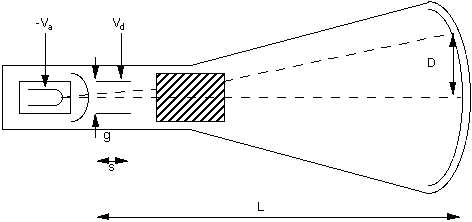
The heart of an oscilloscope is a cathode ray tube (CRT), similar to that in a TV set, in which an electron beam excites a spot on a phosphor screen. The resulting visible spot of light is usually made to draw a graph where the y-axis is the measured signal and the x-axis is time. (But sometimes the x-axis is another signal so that the time behavior of the two can be compared.) An "electrostatic deflection tube" is used in which the electron beam is steered by two sets of plates that apply electric fields to deflect the electron beam in both the horizontal and vertical directions.
The voltage applied between the vertical or Y input and ground is amplified and applied to the vertical plates in the CRT to deflect the electron beam in the vertical direction. The deflection of the beam, and the corresponding deflection of the light spot, are proportional to the applied voltage. It is usually calibrated so that input voltage differences can be read directly from the vertical divisions on the screen according to the scale (amplification or gain) selected by the front panel control (Volts/Cm). This scale should be selected so that the height of the screen represents an amplitude a bit larger than the that of the input signal.
Figure 10.1. Main elements of the Cathode Ray Tube(CRT)
In a similar manner the spot is deflected in the horizontal direction by a voltage applied to the horizontal plates. Usually this voltage is a "ramp" (that is a signal which increases linearly with time) generated internally by the oscilloscope's "time base" or "sweep generator." This sweeps the spot at a uniform, measured rate from the left side to the right side of the screen and then rapidly returns it to the left side to start over. In this way the horizontal position on the screen is proportional to time. The sweep rate is also usually calibrated so that time intervals can be read directly from the horizontal divisions on the screen according to the sweep rate selected by the (horizontal) front panel control (Time/Cm). This rate should be selected so that the width of the screen represents a time interval a bit larger than the duration of the features being investigated.
The result is that the oscilloscope plots out a graph of the input voltage as a function of time on the screen of the CRT. However, there are some practical details which must be understood in order to get satisfactory results. Familiarize yourself with your oscilloscope.
Make sure it is plugged in. Find the controls discussed above. Disconnect any input cables and turn it on. Set it for free-running (or non-triggered) operation ("Auto" position or stability control clockwise); this will be explained below. You should see a horizontal line (the graph of a constant zero volts input). Make sure the vertical and horizontal positions are on the screen and adjust focus and intensity to give a satisfactory display. If necessary to get started, ask your instructor for assistance. Try adjusting the horizontal sweep control (Time/Cm) through its range to observe its effect.
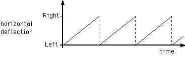
Horizontal
Figure 10.2. Sweep Ramp
If the voltage changes were slow enough then on a very slow sweep speed you could directly see the progress of the spot around the screen. Electronic signals are often too fast to see this way. Besides, it is hard to see signals slower than the persistence of the phosphor because, as the beam moves on, the illuminated trace fades from view; this prevents you from seeing the whole wave form at once.
So, for reasons of practicality and convenience, the spot will usually be moving too rapidly for your eye to follow. What you actually see will be the superposition of multiple successive tracks across the screen. Only if the tracks exactly coincide will the image you see be a single sharp line. Otherwise, it will be rather unintelligible.
This will not be possible unless the input signal is periodic. Even then it will not occur if the period of the signal does not happen to be the exactly the same as that of the sweep (called synchronization). This situation is illustrated in the Figure 10.3.
One way to accomplish synchronization is to adjust either the frequency of the input signal or of the sweep so that they match. This is often hard to do satisfactorily because things tend to drift; besides it may be experimentally inconvenient.
Connect a function generator to an input of the oscilloscope (check that the input channel is turned on). Set it for sine wave output and about 1000Hz frequency with the amplitude control at mid-range. Find the appropriate setting for the time base and the vertical gain. Make sure the oscilloscope is in free-running mode and attempt synchronization both by adjusting the frequency of the signal generator and by using the variable (non-calibrated) sweep rate control. You should observe the situation described above.
A more satisfactory solution to the synchronization problem is provided by "triggered" operation of the oscilloscope. In this mode, rather than having the ramp start over as soon as the previous sweep is finished (called "free-running"), the time base waits to restart the ramp until the input crosses a certain voltage level ("triggers"). As long as this is the same point of the input wave form each time, the sweep across the screen will be synchronized with the repeating signal. This is illustrated in the Figure 10.4.
To use triggered operation, stop the sweep from free-running (set to "Norm" or turn the stability control counter-clockwise to near mid-range). Set the trigger selector to internal and activate the trigger button for the channel from which you want to trigger. Adjust the trigger level to stabilize the display. Observe what happens to the display as you vary the trigger level and change the sign of the trigger selection. (The auto position of the trigger level causes triggering to occur at the mean level of the input wave form.) Change the amplitude of the generator and note how the display changes.
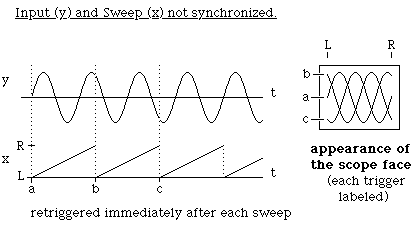
Figure 10.3
Measure the amplitude and frequency of the signal. To do this accurately, the variable controls on the time base and the vertical gain must be in the "cal"(ibrated) position. Observe the square and triangle outputs of the signal generator also.
On Tel equipment scopes only: the stability control allows three modes of triggering. (1) Fully clockwise: triggering occurs continuously (free-running). (2) Fully counterclockwise: no triggering occurs. (3) Midrange: sweep will trigger on the level you set with the trigger level control. Normally this control should adjusted just to the point at which triggering begins.
When using both channels, keep the alt.-chop switch in the alt. position.
Caution:
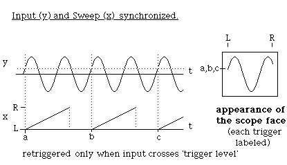
Figure 10.4
Part I: RC Circuits
A capacitor stores electric charge. Typically, a capacitor is made of two parallel plates. Each plate will have a charge of the same magnitude Q but of opposite sign between which there will be an electric field. The work (per unit charge) this field would do on a test charge moved between the plates is the potential difference or voltage V across the plates of the capacitor.
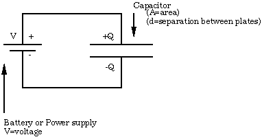
Figure 10.5
The charge and voltage are linearly related by a constant C which measures the capacitance. Consider the situation in which a capacitor is charged by a battery through a resistance as shown below (switch in the charge position). The charge stored on the capacitor (and therefore the voltage across it) increases with time because of the current, which is a flow of charge through the resistance. This current, by Ohm's law, is proportional to the voltage across the resistor,
 . (10.1)
This current will decrease as
 rises toward
 so the rate at which the capacitor is charging up will fall. Eventually, when
there is no further flow of charge the capacitor will be fully charged to its
final value,
so the rate at which the capacitor is charging up will fall. Eventually, when
there is no further flow of charge the capacitor will be fully charged to its
final value,
 . (10.2)
The charge on the capacitor and the voltage across the capacitor do not grow linearly with time. Rather, they follow an exponential law. If the capacitor is initially (at t = 0) discharged this takes the form (see Appendix D on Exponential Decay),
 . (10.3)
After a time t = RC, the capacitor is charged to within,
 ,
,
of the final value. The value RC is known as the time constant of the circuit. If the resistance R is in ohms and the capacitance C is in farads then the time constant RC is in seconds.
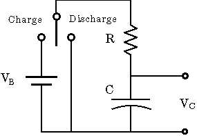
Figure 10.6. RC Circuit
Similarly, if a fully charged capacitor is discharged through a resistance (e.g. by moving the switch to the discharge position) the voltage across the capacitor (and the charge on it) will fall to zero exponentially with time, as shown below,
 . (10.4)
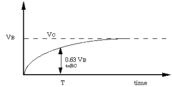
Figure 10.7. Charging a Capacitor through a Resistor
Again, after a time t = RC the capacitor will discharge to 0.63 of its initial value.
In the first part of this experiment you will investigate the charging and discharging of a capacitor for different values of the time constant. By observing the voltage on the capacitor with an oscilloscope you can measure it as a function of time.
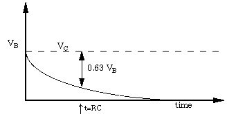
Figure 10.8. Discharging a Capacitor
Although for purposes of illustration it is convenient to discuss charging and discharging the capacitor with a switch, it is experimentally more practical to apply a square wave which duplicates the switch on and off action with a signal generator as shown below.
This is a way of regularly switching the applied voltage between two values so that the capacitor can charge and discharge between them. The charging and discharging traces will be accurately reproducible from cycle to cycle. Then if the oscilloscope is triggered off the periodic input these successive traces will overlay each other on the screen. And the "switching" can occur at a fast enough rate that the result will be a bright, stable display from which you can make measurements. If the period of the square wave is over several time constants the capacitor will approach very close to its final value before the square wave switches.
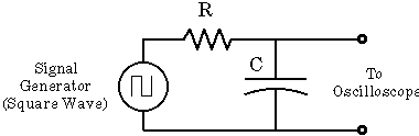
Figure 10.9. RC Test Circuit
Hook up the function generator, set to produce square waves, as above using (variable) resistor and capacitor decade boxes. Find a convenient amplitude and frequency and then look at and trigger on the output of the signal generator. Connect the other channel to observe the capacitor voltage at the same time. You should obtain a display similar to that shown below.
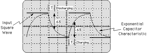
Figure 10.10.
Data sheets are available on which to record your data. (See sample data sheets at the end of this lab). Complete them for the experiments below before you leave and hand them in with your lab report.
Procedure
 ;
C=0.01
;
C=0.01
 and the frequency of the square wave (=3000Hz). Adjust the frequency of the
signal generator for an appropriate display (see figure 10.10) and trace it on
a data sheet. Determine both the charging and discharging time constant by
measuring the time taken for the voltage to change from its initial value to
within 1/e of its final value.
and the frequency of the square wave (=3000Hz). Adjust the frequency of the
signal generator for an appropriate display (see figure 10.10) and trace it on
a data sheet. Determine both the charging and discharging time constant by
measuring the time taken for the voltage to change from its initial value to
within 1/e of its final value.
Questions
Part II: The Forced Damped Oscillator
In this section you will study the electrical version of the mechanical system that you have studied in your mechanics course. There is an exact isomorphism between the two cases as Figure 10.11 indicates.
On the right we have a mass m on a spring of constant k
and with damping b. This is being driven by an oscillating force of
constant amplitude at an angular frequency
 (which can be varied). This system has a resonant frequency,
 . (10.5)
for which the response is a maximum when the driving frequency
 is equal to
 .
In the vicinity of
.
In the vicinity of
 the response curve looks like Figure 10.12, where the width of the curve (
 )
from the point where A =
)
from the point where A =
 =
=
 is given by
 .
There is a demonstration of a mechanical system which your teaching assistant
will show you.
.
There is a demonstration of a mechanical system which your teaching assistant
will show you.
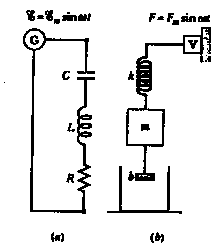
Figure 10.11. (a) is the electrical system, (b) is the mechanical system.
Introduction
In this experiment you will investigate the general phenomenon of resonance in the form of the particular example of an RLC (resistor, inductor and capacitor) circuit. You will be able to determine steady state behavior as well as the Q (quality) factor. In the process you will gain some experience with electronic circuits and components. You will set up the circuit shown in figure 10.13. Be sure that the ground to the signal generator is the same as the voltmeter.
The basic equation that describes the phenomenon of resonance is that of a driven, damped, harmonic oscillator. In the case of the above RLC circuit, this takes the form,
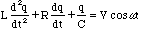 , (10.6)
where q is the charge on the capacitor and V is the peak
amplitude of the signal generator and  is the angular frequency.
It is important to understand that the phenomena are characteristic of the equation and not peculiar to its electrical realization. For instance, if it were a mechanical oscillator the phenomena of resonance would be the same.
Theory on Steady State RLC
The steady state term is,
 , (10.7)
where
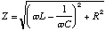 , (10.8)
and
 (10.9)
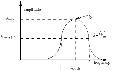
Figure 10.12
The general solution of this equation (written in terms of I = dq/dt, which is
more practical to measure) has two parts,  ,
a steady state and a transient term.
,
a steady state and a transient term.
You are going to measure the RMS voltage
 across the resistor. So
 .
The steady state Is is the term caused by the driving voltage; it is all that
is left after initial transients have died away. The physical significance of
these quantities can be made more apparent by expressing them in terms of the
more universal quantities resonant angular frequency,
.
The steady state Is is the term caused by the driving voltage; it is all that
is left after initial transients have died away. The physical significance of
these quantities can be made more apparent by expressing them in terms of the
more universal quantities resonant angular frequency,
 , (10.10)
and
 , (10.11)
the quality factor Q is roughly the number of oscillations it takes for
the transient to die down. Thus in terms of
 and Q we have,
 , (10.12)
and
 , (10.13)
it is apparent that, in the steady state, at the resonant frequency (
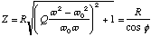
 )
the phase angle will be zero, the circuit will act just like a resistance
R and the current will be maximum. Away from the resonant frequency the
amplitude of the current will decrease. The "full width at half maximum (half
power = .707 of maximum current)" of the resonance curve will be about,
)
the phase angle will be zero, the circuit will act just like a resistance
R and the current will be maximum. Away from the resonant frequency the
amplitude of the current will decrease. The "full width at half maximum (half
power = .707 of maximum current)" of the resonance curve will be about,
 , (10.14)
that is it will be narrower, in terms of a fraction of the resonant frequency, directly as Q increases.
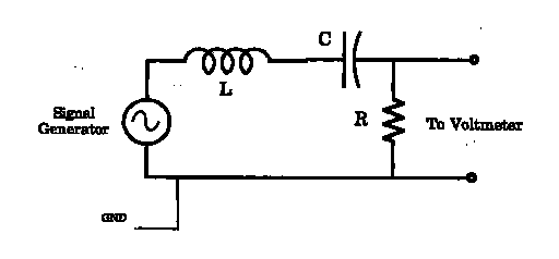
Figure 10.13. A Driven RLC Circuit
Procedure
Assemble the experimental circuit above using the values:


 .
Set the oscillator frequency f near the value calculated. The
oscillator voltage should be set at around 3 Volts.
.
Set the oscillator frequency f near the value calculated. The
oscillator voltage should be set at around 3 Volts.
 .
This frequency will probably be a little different from your calculation. You
do not need the oscilloscope for this part of the experiment. The curve near
.
This frequency will probably be a little different from your calculation. You
do not need the oscilloscope for this part of the experiment. The curve near
 should look like that in figure 10.12 Take measurements of V in the vicinity of
 ,
two measurements below and above will be sufficient.
,
two measurements below and above will be sufficient.
 and repeat the measurements.
 and repeat the measurements. At this point you have done three sets of
measurements.
and repeat the measurements. At this point you have done three sets of
measurements.
 .
Now find the resonant curve. Is the resonant frequency one half of what it was
in the above experiments?
.
Now find the resonant curve. Is the resonant frequency one half of what it was
in the above experiments?
 .
.
 and repeat. (You should have six data sets.)
Data Analysis
 of each of the curves.
 ?
?
 ,
L=100mH data.
,
L=100mH data.
Name:____________________________________
Data Sheet for known:

______________________seconds(measured T charging)
______________________seconds(measured T discharging)
______________________ohms
R
______________________ohms
C
______________________ohms
RC
Date:_________________________
Name:____________________________________
Data Sheet for known: 30% values

______________________seconds(measured T charging)
______________________seconds(measured T discharging)
______________________ohms
R
______________________ohms
C
______________________ohms
RC
Date:______________________________
Name:__________________________________
Data Sheet for unknown C

______________________seconds(measured T charging)
______________________seconds(measured T discharging)
______________________ohms
R
______________________ohms
C
______________________ohms
RC
Date:_________________________
Name:____________________________________
Data Sheet for unknown R

______________________seconds(measured T charging)
______________________seconds(measured T discharging)
______________________ohms
R
______________________ohms
C
______________________ohms
RC
Name:_____________________________
Initial Values:

Frequency Voltage
Name:_____________________________
Initial Values:

Frequency Voltage
Name:_____________________________
Initial Values:

Frequency Voltage
Name:_____________________________
Initial Values:

Frequency Voltage
Name:_____________________________
Initial Values:

Frequency Voltage
Date:______________________________
Name:_____________________________
Initial Values:

Frequency Voltage
Data
Sine Wave
(Suggested values for RLC in Resonance)
Capacitance Resistance Inductance Frequency
(nF) (K ) (mH) (KHz)
Max .043nF 3K
) (mH) (KHz)
Max .043nF 3K 30mH 105KHz
Min .028nF
Max .326nF 13K
30mH 105KHz
Min .028nF
Max .326nF 13K 30mH 250KHZ
Min .046nF
Max .058nF 3K
30mH 250KHZ
Min .046nF
Max .058nF 3K 30mH 90KHz
Min. .030nF
Max .264nF 3K
30mH 90KHz
Min. .030nF
Max .264nF 3K 25mH 70KHz
Min .036nF
Max .392nF 3K
25mH 70KHz
Min .036nF
Max .392nF 3K 50mH 50KHz
Min .048nF
Max .32nF 3K
50mH 50KHz
Min .048nF
Max .32nF 3K 100mH 25KHx
Min .04nF
Max .321nF 3K
100mH 25KHx
Min .04nF
Max .321nF 3K 100mH 15KHz
Min .041nF
Max .323nF 3K
100mH 15KHz
Min .041nF
Max .323nF 3K 100mH 25KHz
Min .041nF
Max .327nF 3K
100mH 25KHz
Min .041nF
Max .327nF 3K 100mH 80KHz
Min .043nF
100mH 80KHz
Min .043nF
Square Wave
Capacitance Resistance Inductance Frequency
(nF) (K ) (mH) (KHz)
unchanged 13K
) (mH) (KHz)
unchanged 13K & up unchanged 1.5KHz
unchanged 52K
& up unchanged 1.5KHz
unchanged 52K & up unchanged 2.3KHz
unchanged 20K
& up unchanged 2.3KHz
unchanged 20K & up unchanged 2.4KHZ
unchanged 13K
& up unchanged 2.4KHZ
unchanged 13K & up unchanged 1.1KHZ
unchanged 13K
& up unchanged 1.1KHZ
unchanged 13K & up unchanged 8KHz
unchanged 13K
& up unchanged 8KHz
unchanged 13K & up unchanged 2KHz
unchanged 13K
& up unchanged 2KHz
unchanged 13K & up unchanged .3KHz
unchanged 13K
& up unchanged .3KHz
unchanged 13K & up unchanged .8KHz
unchanged 13K
& up unchanged .8KHz
unchanged 13K & up unchanged .9KHz