Time Equalizer Board
Prototype Test
W.S. Aug/21/01
Abstract: The Time Equalizer board is under development. This
single width CAMAC unit will be used to align timing signals from the Cerenkov
counters (either the Maryland Cerenkov array or Rochester T0's) for the
PHOBOS experiment at RHIC.
Design goals
Date: Fri, 13 Apr 2001 16:05:46 -0400 (EDT)
From: Wojtek Skulski <skulski@phobtof.pas.rochester.edu>
To: Frank Wolfs <wolfs@pas.rochester.edu>,
PHOBOS TOF Group <tof@liststar.pas.rochester.edu>
Board form factor
CAMAC single width
Number of channels
16
Signal in and out
ECL
Connectors
ribbon cable, two connectors (in and out)
Shortest possible delay tpd 6.5 ns
Shortest possible delay step 10 ps
Number of steps
256
Longest possible delay
1 milisecond
Delay tempco
7.5 ps/degree C
Delay jitter
10 ps
Single step size
settable by swapping resistors
Max trigger rate per channel 60 MHz
Min output pulse width
3 ns
Max output pulse width
several ns (set once per chip with a R/C)
Remarks:
1. The total delay is given by
td = tpd
+ N*(range/256) N = 0,1,2,...,255
i.e., the delay range is divided into 256 equal steps. There
is a
minimum propagation delay tpd of 6.5 ns.
The step size of 10 ps is only applicable at the shortest
range of 2.5 ns.
At longer ranges the step size will be longer. For example,
if the range
is set to 25 ns, then the step size will be 100 ns, and
the total
delay will be 6.5 ns to 31.5 ns.
The schematic and the board layout
Both the schematic and the board layout were done during off-shift hours
in the TOF apartments, both on-site and at the NAT Center. I appreciate
the patience of my roommates while I was working on the board. Jan Toke
of the Rochester Nuclear Chemistry group reviewed the schematic and pointed
out a couple of mistakes
In order to achieve the design goals I used layout techniques appropriate
for high-speed analog design, such as four-layer printed circuit board
with separate power and ground planes. A few components, such as pull-up
resistors and a DIP-switch, are meant only for initial testing without
the benefit of a full-blown CAMAC interface, which will be assembled at
a later stage.
The prototype
The prototype PCB was produced by Sierra
Proto Express, whose web site can be reached under a funny name www.2justforyou.com.
Despite the funny name, their service was quick and very professional.
I was more than pleased with both the price and the quality of the PCBs.
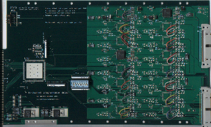
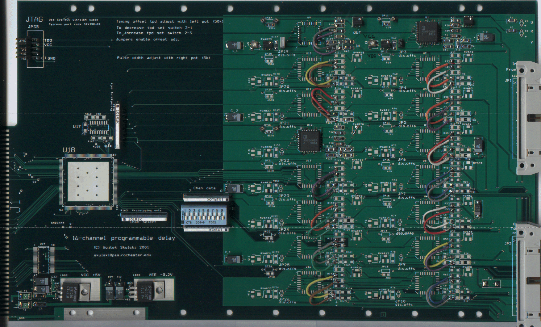
Figure 1. (Click here
to
see a more detailed photo). The actual prototype with two delay chips soldered
in (black rectangles near the upper-right corner and in the center of the
board). The input/output ribbon cable sockets are on the right, the CAMAC
connector is on the left. The wire loops soldered in other channels were
used to measure the input-output propagation time for the unpopulated channels.
The blue DIP switch was used to dial in the value of the delay during the
tests. The silver square on the left is the area where the CAMAC interface
chip will be soldered.
I soldered the surface-mount chips, resistors,
and capacitors myself. The soldering of the 28-pin delay chips in PLCC
packages was a bit tricky. The pins of those chips are tucked under the
chip body like a letter "J", what is not really meant for hand soldering.
The first test
The first tests were performed on Aug/16, using a NIM pulser, ECL-NIM-ECL
converters, a TAC, and an ADC. Only one channel out of sixteen was
populated with components. The time range of the delay chip was set to
2.5 ns using a socketed resistor.
Date: Fri, 17 Aug 2001 12:33:00 -0400 (EDT)
From: Wojtek Skulski <skulski@phobtof.pas.rochester.edu>
To: PHOBOS TOF Group <tof@liststar.pas.rochester.edu>
Subject: Equalizer board tests
The sigma contribution of the board itself (disentangled
from the data) is 5.2 ps. This number is in fact 3 times
smaller than the TAC channel width in this measurement.

Figure 2. (The picture size was shrunk, what
may have introduced a distortion. Click here
for the full-size picture). The sequence of peaks corresponding to the
delay word = 0, 64, 128, 192, 255. The left-most peak was acquired with
the board bypassed (inputs shorted to outputs). The minimum propagation
delay equal to 6.6 ns is indicated with a horizontal arrow.
The very small jitter introduced by the board is evidenced by a slight
increase of the width of the peaks, as compared with the left-most one.
The reference peak without the board is only 2 ADC channels wide. The board
adds one more channel to the width. This is consistent with the specs of
the delay chip, which specifies resolution of one delay step = 10ps (in
the present case 2.5ns / 255 steps). From the direct comparison of the
spectra we see that the increase in the width is indeed consistent with
one delay step.
Fitting such narrow peaks with a gaussian is only approximate. Therefore,
the exact value of the board's time jitter equal to 5.2 ps (one sigma)
should be treated with a grain of salt. More importantly, the width of
the time peaks is entirely consistent with the intended use of the board.
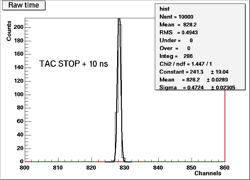
Figure 3. The reference peak (with the board
bypassed) is less than 2 channels wide.
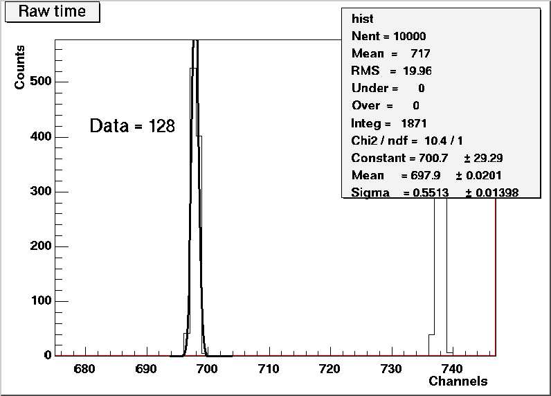
Figure 4. The width of the peak after delaying
by the board has increased by about one TAC channel, i.e., 15 ps. The increase
in "sigma" of the peak is about 5 ps.
The CAMAC interface
After completion of the tests described above I soldered the CAMAC interface
chip (a PQFP package with 208 pins). I used a 15-watt soldering iron from
Radio Shack, which performed surprisingly well for its price of $9. Send
me an e-mail if you are interested in details, because there are a few
tricks to pay attention to when soldering such chips.
The chip was then programmed over the JTAG port with the help of the
Cypress ISR cable. The CAMAC interface worked right out of the box. Two
small mistakes in the interface logic were identified and corrected, and
the chip was reprogrammed with a new version of the CAMAC interface logic.
The board responds to two CAMAC commands: F(16)Ax to set the delay word
for the channel "x", x=0..15, and F(0)Ax to read the programmed delay word
from channel "x". The CAMAC commands are the same as in the case of
CAMAC discriminators. This will facilitate writing the Labview GUI.
The conclusion and the plans
The tests indicate that the equalizer board will perform its statutory
duty. Several things need to be done:
-
Assemble and debug the CAMAC interface using the current prototype (done,
see above).
-
Add a hardware OR to the board layout.
-
Procure and test the 2nd (and hopefully final) version of the PCB.
-
Assemble and test the actual production boards.
-
Modify the Labview interface to interact with the board(s) to be installed
in the tunnel.
-
Install the appropriate number of the boards in the tunnel, connect to
the Cerenkov and/or T0 detectors.
-
Comission the whole system.
Questions? Comments? Send an e-mail to skulski@pas.rochester.edu .
Back to top of this page | Back
to PHOBOS home page.
(C) Wojtek Skulski 2001.